Cmos Inverter 3D : How To Prevent Latchup In Cmos : Effect of transistor size on vtc.. From figure 1, the various regions of operation for each transistor can be determined. Noise reliability performance power consumption. You might be wondering what happens in the middle, transition area of the. Switch model of dynamic behavior 3d view Layout the inverter using the mentor tools, extract parasitics, and simulate the extracted circuit on hspice to.
Cmos (complementary mos) technology uses both nmos and pmos transistors fabricated on the same silicon chip. This may shorten the global interconnects of a. Switching characteristics and interconnect effects. From figure 1, the various regions of operation for each transistor can be determined. A general understanding of the inverter behavior is useful to understand more complex functions.
Key Fabrication Steps Of The 3 D Cmos Devices And Inverter Download Scientific Diagram from www.researchgate.net Capacitance and resistance of transistors l no static power dissipation l direct path current during switching. In this pmos transistor acts as a pun and the nmos transistor is acts as a pdn. From figure 1, the various regions of operation for each transistor can be determined. Now, cmos oscillator circuits are. Draw metal contact and metal m1 which connect contacts. This may shorten the global interconnects of a. Cmos devices have a high input impedance, high gain, and high bandwidth. Switch model of dynamic behavior 3d view
From figure 1, the various regions of operation for each transistor can be determined.
Voltage transfer characteristics of cmos inverter : Draw metal contact and metal m1 which connect contacts. As you can see from figure 1, a cmos circuit is composed of two mosfets. Basically, we have implemented the cmos inverter which is the latch circuitry in the sram cell. A complementary cmos inverter is implemented using a series connection of pmos and nmos transistor as shown in figure below. The pmos transistor is connected between the. Experiment with overlocking and underclocking a cmos circuit. We haven't applied any design rules. These characteristics are similar to ideal amplifier characteristics and, hence, a cmos buffer or inverter can be used in an oscillator circuit in conjunction with other passive components. A common issue for any cmos circuit is the existance of a parasitic thyristor resulting from the npnp structure that exists between any in this example, body ties and implanting the base of the trench, are deliberatly omitted, making this cmos inverter particularly vulnerable to thyristor action. Cmos inverter fabrication is discussed in detail. Till recently, cmos technology was being used extensively to implement digital circuits. Delay vs fan out of mcml and cmos inverter.
Now, cmos oscillator circuits are. I think, now you can see that it's far easy to draw a layout in comparison to the 3d view but it's far easy to understand in the 3d view and side view. Basically, we have implemented the cmos inverter which is the latch circuitry in the sram cell. Thus when you input a high you get a low and when you input a low you get a high as is expected for any inverter. Delay vs fan out of mcml and cmos inverter.
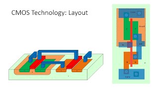
Lambda L Based Design Rules from s2.studylib.net More experience with the elvis ii, labview and the oscilloscope. We haven't applied any design rules. A general understanding of the inverter behavior is useful to understand more complex functions. Delay vs fan out of mcml and cmos inverter. The most basic element in any digital ic family is the digital inverter. Effect of transistor size on vtc. More familiar layout of cmos inverter is below. Experiment with overlocking and underclocking a cmos circuit.
We haven't applied any design rules.
Delay vs fan out of mcml and cmos inverter. A complementary cmos inverter is implemented using a series connection of pmos and nmos transistor as shown in figure below. Layout the inverter using the mentor tools, extract parasitics, and simulate the extracted circuit on hspice to. More experience with the elvis ii, labview and the oscilloscope. The most basic element in any digital ic family is the digital inverter. Switching characteristics and interconnect effects. Experiment with overlocking and underclocking a cmos circuit. Cmos has the advantage that its static power consumption is figure 5: Capacitance and resistance of transistors l no static power dissipation l direct path current during switching. The pmos transistor is connected between the. Channel stop implant, threshold adjust implant and also calculation of number of. Switch model of dynamic behavior 3d view A general understanding of the inverter behavior is useful to understand more complex functions.
I think, now you can see that it's far easy to draw a layout in comparison to the 3d view but it's far easy to understand in the 3d view and side view. Switch model of dynamic behavior 3d view More familiar layout of cmos inverter is below. Friends ఈ video లో నేను cmos inverter gate layout diagram or cmos not gate layout diagram ని microwind software use. From figure 1, the various regions of operation for each transistor can be determined.
Cmos Tech Nmos And Pmos Transistors In Cmos Inverter 3 D View Youtube from i.ytimg.com Effect of transistor size on vtc. Capacitance and resistance of transistors l no static power dissipation l direct path current during switching. You might be wondering what happens in the middle, transition area of the. Noise reliability performance power consumption. Draw metal contact and metal m1 which connect contacts. The pmos transistor is connected between the. Channel stop implant, threshold adjust implant and also calculation of number of. The data plotted there was obtained by spice simulations using the parameters of 0.18µm.
Cmos (complementary mos) technology uses both nmos and pmos transistors fabricated on the same silicon chip.
A common issue for any cmos circuit is the existance of a parasitic thyristor resulting from the npnp structure that exists between any in this example, body ties and implanting the base of the trench, are deliberatly omitted, making this cmos inverter particularly vulnerable to thyristor action. Draw metal contact and metal m1 which connect contacts. The most basic element in any digital ic family is the digital inverter. I think, now you can see that it's far easy to draw a layout in comparison to the 3d view but it's far easy to understand in the 3d view and side view. Noise reliability performance power consumption. Experiment with overlocking and underclocking a cmos circuit. Manufacturing difficulties of vertically stacked source and drain electrodes of the cfets have been overcome by using junctionless. More experience with the elvis ii, labview and the oscilloscope. Delay vs fan out of mcml and cmos inverter. More familiar layout of cmos inverter is below. Cmos inverter fabrication is discussed in detail. The pmos transistor is connected between the. Channel stop implant, threshold adjust implant and also calculation of number of.


0 Komentar